
Design FFT circuit

1. Purpose
The Fourier transform has been widely used in the field of digital signal processing. This method is also utilized to demodulation of OFDM receiver side. In wireless communication systems, we must change the number of the fixed data point which use the Fourier transform, and we must also change it to obey the standards. We would like to change from the fixed data point to the variable data point. As a reason, we are troublesome that we change the fixed data point by every standard. The purpose of this text is we design FFT circuit.
2. Design Environments
MATLAB 7.9.0 (R2009b) XILINX®System Generator for DSP 12.1
3-1. Discrete Fourier Transform
DFT (Discrete Fourier Transform) is the fourier transform on the discrete time domain, and this method is often used for the frequency analysis of a discrete digital signal in the digital signal processing. Now, we perform the frequency analysis of discrete time domain signal x[n] ( x[n] is complex values).
We obtain the N-sample signal in frequency domain (complex values) X[0], … , X[N-1] which use DFT to the N-sample signal in time domain x[0], … , x[N-1].
Using the twiddle factor , the discrete Fourier coefficients are expressed as equation (1.2)
The case of N=4 is shown using the matrix representation in equation (1.3).

Calculating equation (1.3) results are as following equations (1.4) ~ (1.7).
According to equations (1.4) ~ (1.7), the N=4 DFT requires 16 times complex multipliers, and 12 times complex adders. Similarly, the N-point DFT requires N2 times complex multipliers, and N(N-1) times complex adders. The most of processing time which calculate the DFT using computer is the calculation time of the complex multipliers. If the number of complex multipliers is significant reduced, the processing speed of the DFT is expected to increase significantly.
3-2. Fast Fourier Transform
FFT (Fast Fourier Transform) is an algorithm, which speeds up the calculation of the discrete Fourier transform. It was proposed by John James Cooley in 1965.
The algorithm is described as follows
For example, in case of N=4, the matrix representation of the discrete Fourier coefficients is shown as equation (1.3).
By even-odd sorting the index of the input column X[k], the following eq. (2.1) is obtained

Here, we consider about the property of the twiddle factor. The twiddle factor has the periodic property as be shown in equation (2.2)

The proof of equation (2.2) is as follows.
The left-side of equation (2.2) is rewritten as following equation:
The N power of the twiddle factor ![]() is :
is :

According to the Euler’s identity ![]() , we have
, we have![]()
Accordingly,
Therefore,
Calculating in the same way, the N/2 power of the twiddle factor ![]()
Therefore,
Equation (2.1) is represented by using the periodic property of the twiddle factor ![]() as follow:
as follow:

This matrix decomposes (2.4) because coefficient matrix (2.3) has the regularity.

Decomposed coefficient matrix (2.4) can change as follows.

O is 2×2 zero matrix I is 2×2 identity matrix
We calculate of red part in (2.5).

Proceed with further calculations become to (2.7).

Expand (2.7)
Calculated result (2.9),(2.10),(2.11),(2.12) correspond to discrete fourier transform result (1.4),(1.5),(1.6),(1.7) use of periodicity of the twiddle factors.
DFT of N =4 needs 16 times complex multiplier and 12 times complex adder. However, in the case of (2.8) can do 4 times complex multiplier and 4 times complex adder. This algorithm is called fast fourier transform. It is specially lower complex multiplier than DFT.
Radix-2 algorithm
3. Radix-2 algorithm
We talk about Radix-2 algorithm and butterfly computation. It shows fourier transform result of X(k) in last chapter.
Their formulas are coordinated of even or odd at sigma, as (3.1)
One FFT can divide two FFT at N even and N odd.

NIf N is power of 2, it can divide FFT and more. Finally, it divide several FFT(butterfly computation) of N=2. This is Radix-2 algorithm. Its algorithm usually reduce of calculation, reason of using complex adder-subtractor only.
Fig.1 shows butterfly computation circuit using of butterfly computation.
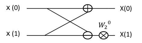 Fig.1: Butterfly computation circuit
Fig.2 shows calculation flow about discrete fourier coefficient of N =4. Note,
under the arrow of -1 is subtraction, twiddle factor at the top of line is multiplication.
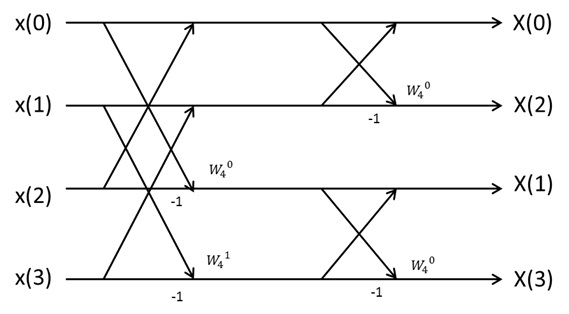 Fig. 2: Conceptual diagram of 4 points FFT about Radix-2 algorithm
Calculated results used of ![]() are changed (3.3) ,(3.4), (3.5), (3.6). Their results equal DFT results.
are changed (3.3) ,(3.4), (3.5), (3.6). Their results equal DFT results.
4-1-1. FFT circuit : N=4
(1) Circuit design
Basic concept of 4 points FFT circuit which applies Radix-2 architecture is shown in figure 3.
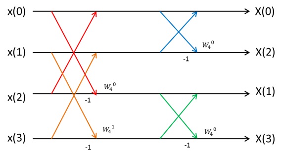 Figure 3: Basic concept of 4 points FFT circuit
In figure 3,4 point FFT circuit can implement by using 4 butterfly processing elements.
Block diagram is shown in figure 4.
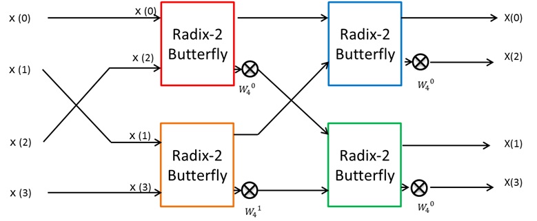 Figure 4: 4 points FFT circuit block diagram
In figure 3, butterfly processing element that is shown red line make be corresponding to red block in figure 4. Another butterfly processing element is same.
This is the 4 points FFT circuit for parallel input.
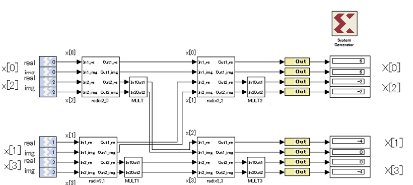 Figure 5: Design of 4 points FFT circuit for parallel input
The detail of each subsystem is shown below
a)radix2
In this part, we explain the Radix2_0, Radix2_1, Radix2_2 and Radix2_3 This circuit has 2 complex number inputs and 2 complex outputs. Therefore, real number and complex number must be separate input, and calculate each part. Architecture is shown figure 4.
Subsystem radix-2_1, radix-2_2, radix-2_3 is same as radix2_0.
 Figure 6: The model of subsystem radix-2_0
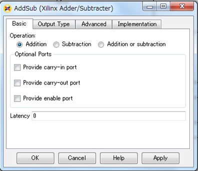
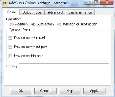 Figure 7: Parameter of AddSub Figure 8: Parameter of AddSub2
AddSub1 in figure 6 is same as AddSub.
AddSub3 is also same as AddSub2.
b) MULT
This section shows the MULT to the MULT3 subsystem. The MULT subsystem multiplies a twiddle factor. The Complex number operation ![]() mutiple
mutiple ![]() is showed by
is showed by
As following this process, multiple twiddle factors in terms of complex input. figure 9 shows the circuit block of the MULT subsystem. Abbreviate explanations of the MULT1 subsystem to the MULT3 subsystem, because of the same architecture as the MULT subsystem against the constant block, the W_real and the W_imag of figure 9, parameters.
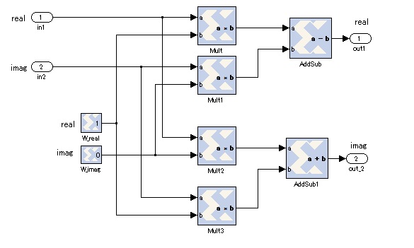 Figure 9: Architecture of the MULT subsystem
Abbreviate an explanation of the AddSub block, because of the same as the AddSub2 block of figure 6.
Also, abbreviate an explanation of the AddSub1 block, because of the same as the AddSub1 block of figure 6.
Figure 10 shows parameters of the Mult block.
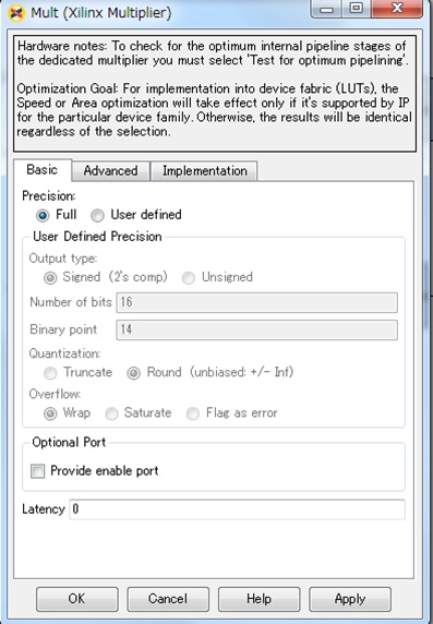
Abbreviate explanations of the Mult1 block, the Mult2 block and the Mult3 block, because of the same parameters as the Mult block of figure 9.
Table 1 shows the Constant block parameters showing the twiddle factors depending on ![]() or
or![]() in the MULT subsystem, the MULT1 subsystem, the MULT2 subsystem and the MULT3 subsystem.
in the MULT subsystem, the MULT1 subsystem, the MULT2 subsystem and the MULT3 subsystem.
Table 1: Parameter of the twiddle factor

The subsystem MULT multiplies the complex twiddle factor in terms of the complex input signals.
(2) Verification
Input x[0] to x[3] of Table 2 into the FFT circuit of Fig.5, then got X[0] to X[3] of Table 2.
figure 11 shows the result of hardware simulation is consistent with the result of MATLAB simulation.
Table 2: Verification Result and Error on MATLAB

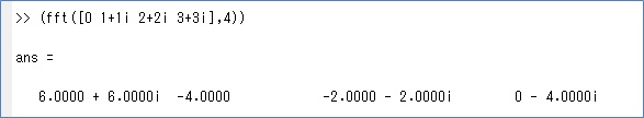 Figure 11: Calculation Result of FFT on MATLAB
Then, figure 12 and figure 13 shows the waveform of input signals and output signals.
Depending on this figure, in case of parallel input, FFT has no latency.
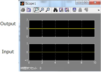
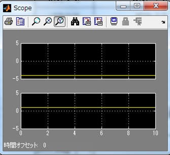 Figure 12: X[0]_real and x[0]_real Figure 13: X[1]_real and x[1]_real
4-1-2. FFT circuit : N=8
(1) Circuit design
As in the case with N=4, design block diagram from the algorithm of 8-point FFT.
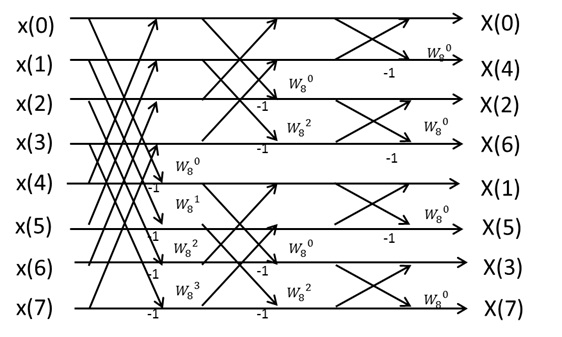 Figure 14: Algorithm of 8 point-FFT
Following the algorithm, 12 of the Butterfly computation circuit construct the N=8 FFT circuit.
Figure 15 shows block diagram.
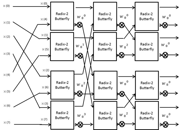 Figure 15: Block Diagram of 8 point-FFT
The designed circuit is shown in figure 16.
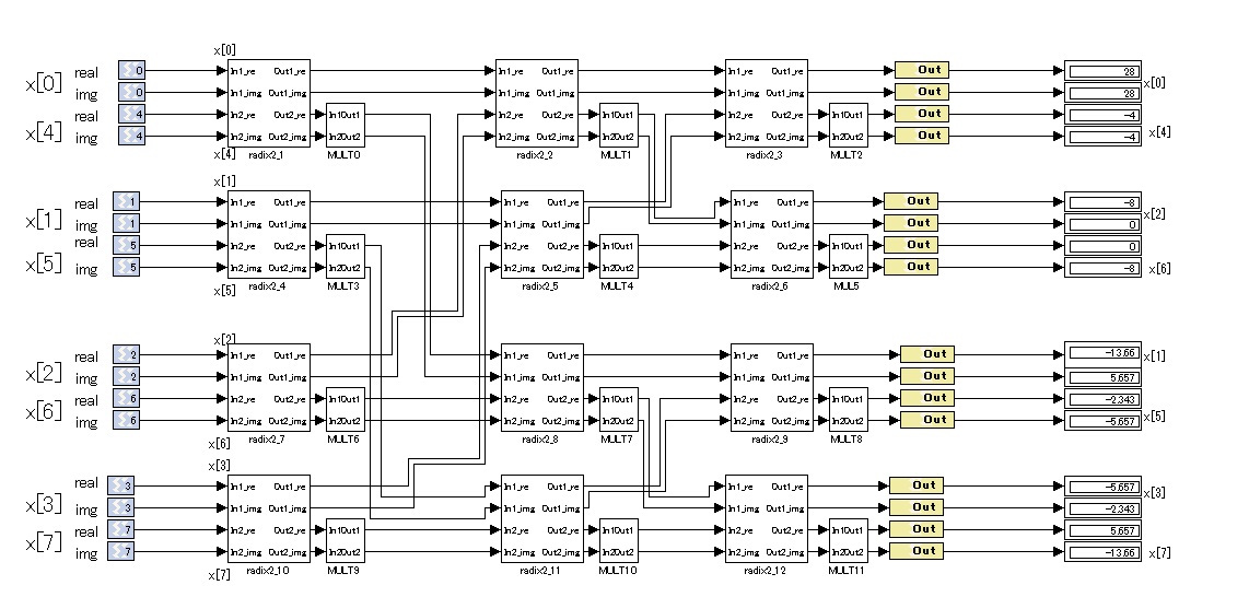 figure 16: 8 point FFT circuit for parallel input
We omit the description of subsystems radix2_1-radix-2_12, because they have the same circuit construction as the subsystem radix-2_0 in figure 6.
We also omit the description of subsystems MULT0-MULT11, because they have the same circuit construction as the subsystem MULT in Figure 7, except for the parameters of constant block.
The parameters of constant block in MULT0-MULT11 are shown in Table 3, where the twiddle factors are![]() 、
、 ![]() 、
、 ![]() 、
、 ![]()
Table 3: Parameters of twiddle factors
![]()
On MULT3 and MULT9 in Table3, we set 0.7071 as a round number for
(2) Notes about fixed-point arithmetic
The bit width of constant blocks of the subsystem MULT is 16-bit, and the fractional bit is 14-bit. ![]() can be expressed as 0.70709228515625 by the fractional bit.
can be expressed as 0.70709228515625 by the fractional bit.
If we design circuits with floating-point arithmetic, the scale of circuits becomes very large. Therefore, fixed-point arithmetic is generally used for calculations. However, in this case, error occurs due to constraints on bit width.
(3)Verification
In figure 9, we simulate the behavior of the circuit. The input signals are x(0)=0+0j, x(1)=1+1j, x(2)=2+2j, x(3)=3+3j, x(4)=4+4j, x(5)=5+5j, x(6)=6+6j, x(7)=7+7j , then the output signals become X(0)=28+28j, X(1)=-13.64+5.678j, X(2)=-8+0j, X(3)=-5.635-2.365j, X(4)=-4-4j, X(5)=-2.3650-5.678j, X(6)=0-8j, X(7)=5.635-13.64j, and Input to Output latency of this circuit is 0.
The difference between the result of circuit simulation and MATLAB simulation is shown in Table The error range is about ![]() , and the cause of this error is rounding error which occurs by expressing
, and the cause of this error is rounding error which occurs by expressing ![]() in binary at constant block of MULT. In order to do more accurate calculation, we need larger bit width for fractional bit of constant block in the subsystem MULT.
in binary at constant block of MULT. In order to do more accurate calculation, we need larger bit width for fractional bit of constant block in the subsystem MULT.
Table 4: The difference between the result of circuit simulation and MATLAB simulation

4-2-1. Design of FFT circuit for serial input
(1) Circuit design in the case of N=4
In chapter A-1, we designed 4 point FFT circuit for parallel input.
The FFT circuit for parallel input can be designed easily, and it has an advantage that Input to Output latency is 0. However the circuit scale becomes very large.
If we designed FFT circuit with less butterfly circuits by reusing them with delay blocks and multiplexer (MUX) blocks, we could make the circuit scale smaller.
In this chapter, we design 4 point FFT circuit for serial input.
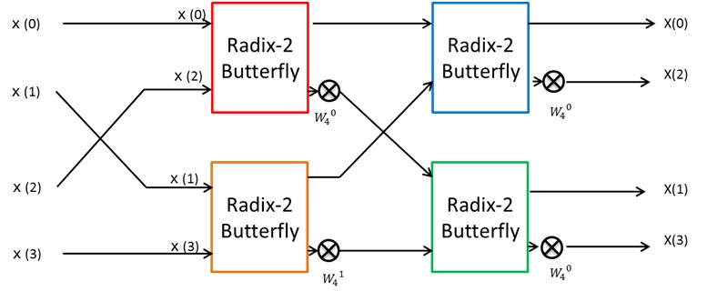 Figure 17: 4 point FFT circuit for parallel input
The conceptual block diagram is as follows.
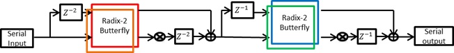 Figure 18: Block diagram of 4 point FFT circuit for serial input.
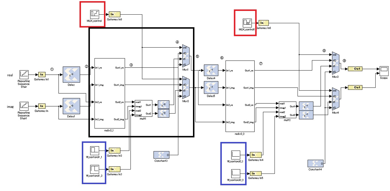 Figure 19: 4 point FFT circuit for serial input
The details of MUX_control and W_control blocks in Figure 19 is described as follows.
a) MUX_control
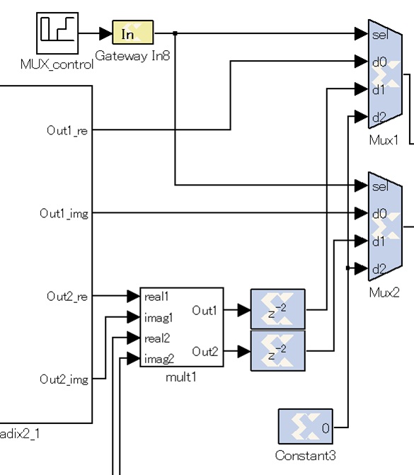 Figure 20: Enlarged view around MUX_control
MUX1 and MUX2 output the values of d0 ~ d2 when sel=0~2. MUX_control decides the output signal of MUX1 and MUX2 multiplexers from d0 ~ d2
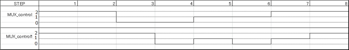 Figure 21: The chart of MUX_contol
The output signal of MUX_control is variable at each step. Therefore, MUX_control can select the signal which is input to next butterfly circuit.
b) W_control
W_control decides the twiddle factor W.
This architecture computes butterfly operation changing the value of twiddle factor W (real part, imaginary part) at each step.
Each block parameters are shown in Table 5.
Table 5: W_control block paramters

From this table, MULT1 block operates multiply by ![]() at first step and
at first step and ![]() at next step. MULT2 block always operates multiply by
at next step. MULT2 block always operates multiply by ![]()
The timing chart of 4-points FFT circuit for serial input signal is shown in Fig. 22.
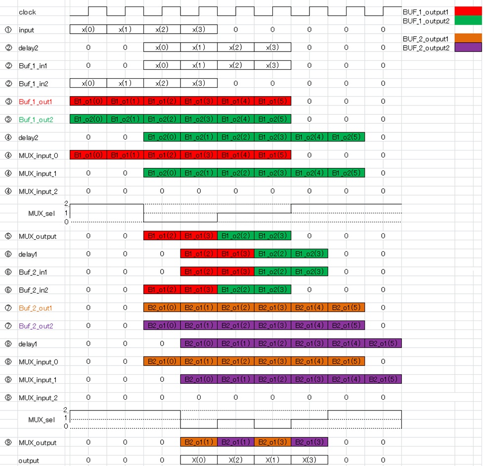 Figure 23: The timing chart of 4-points FFT circuit for serial input signal
(2) Verification
simulation result of this architecture using x(0)=0+0j, x (1)=1+1j, x(2)=2+2j, x(3)=3+3j as input signal is shown in Fig. 23.
 Figure 24: The output signal of 4-point FFT circuit for serial input signal
From this figure, the output signal of this architecture is X(0)=6+6i, X(1)=-4+0i, X(2)=-2-2i, X(3)=0-4i which is same as the MATLAB simulation result (Table 6).
Table 6: The comparison between circuit and MATLAB

And latency of this architecture is 3 clocks.
 Figure 25: MATLAB simulation result
4-2-2. FFT circuit : N=8
(1) Circuit design
 Figure 15: The block diagram of 8-point FFT circuit for parallel input signal
First, the way of 8-point FFT circuit design is explained as follow.
This architecture inputs serial input signal to butterfly operation circuit. The output signals of butterfly operation circuit are selected to compute next butterfly operation by multiplexer.
This circuit is shown in figure 27.
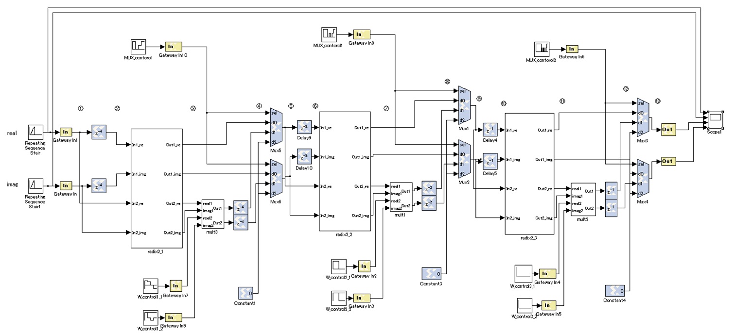 Figure 27: 8-point FFT circuit to the serial input
a) MUX_control
The MUX_control block is a sequence that controls the signal input to the selector of the multiplexer. This signals that determine the output of the multiplexer.
In figure 28, we shows the parameter of sequence.
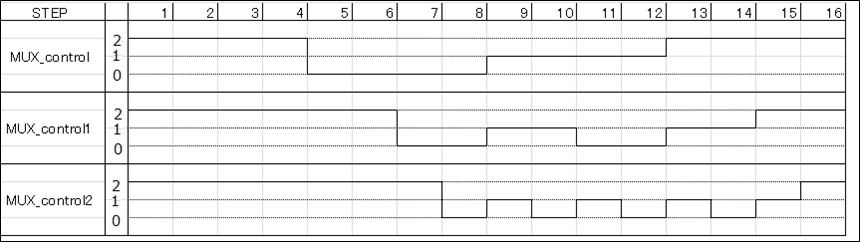 Figure 28: Parameters of the MUX_control sequence
In figure 28, we confirmed that MUX_control value output from each step has been changed. Only the signals required for the FFT butterfly computation circuit of output signal is controlled sent to the next butterfly computation circuit.
b) W_control
W_control is a sequence represented the rotation factor W
By varying the value of the complex twiddle factors are multiplied per STEP, butterfly computation is performed.
The complex twiddle factor is ![]() ,
, ![]() ,
, ![]() ,
, ![]() In Table 7, we shows the parameter of sequence.
In Table 7, we shows the parameter of sequence.
Table 7: Parameters of the W_control sequence

In Table 7, we used the ![]() is as approximate number 0.7071.
is as approximate number 0.7071.
In Tabel 7, we confirmed multiply the first step in ![]() , in MULT0 of the figure 26, since then, in turn multiplied by
, in MULT0 of the figure 26, since then, in turn multiplied by ![]() ,
, ![]() ,
, ![]() , The first step in MULT1 multiplies the
, The first step in MULT1 multiplies the ![]() the next step is to multiply the
the next step is to multiply the ![]() The MULT2 are always multiplied by the
The MULT2 are always multiplied by the ![]()
In figure 27, we show the 8-point FFT circuit timing chart of figure 29 for the serial input.
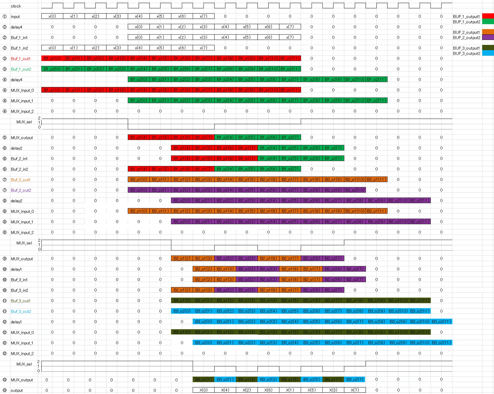 Figure 29: 8-point FFT circuit timing chart for the serial input
(2) Evaluation
Because it is hard to recognize the value of under decimal point from output wave shown by figure 26, we show those values on MATLAB. x(0)=0+0j, x(1)=1+1j, x(2)=2+2j, x(3)=3+3j, x(4)=4+4j, x(5)=5+5j, x(6)=6+6j, x(7)=7+7j Output signals are
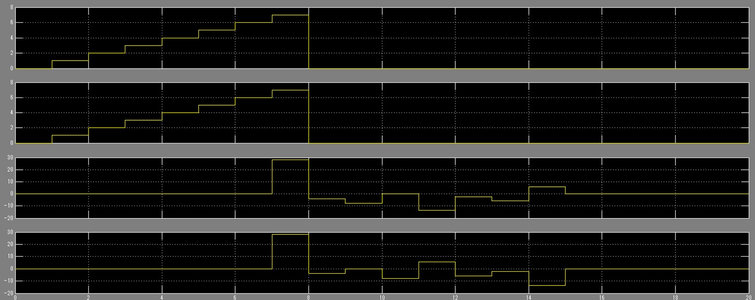 Figure 30: 8-point FFT circuit on the output signal of the serial input
In Figure 30, as will be noted from the Table 8, first step on MULT0 is multiplying by X(0)=28+28j, X(1)=-13.6570+5.6575j, X(2)=-8+0j, X(3)=-5.6570-2.3430j, X(4)=-4-4j, X(5)=-2.3430-5.6575j, X(6)=0-8j, X(7)=5.6570-13.6570j
The deference between above values and the results calculated on MATLAB (Figure 27) is shown by table 8.
Maximum error is, ![]() A reason of this error is Round-off Error caused by representing
A reason of this error is Round-off Error caused by representing ![]() with binary .
with binary .
Table 8: Error compared to calculated results on MATLAB

 Figure 31:&Calculated results on MATLAB
4-2-3. FFT circuit : N=16
(1) Circuit design
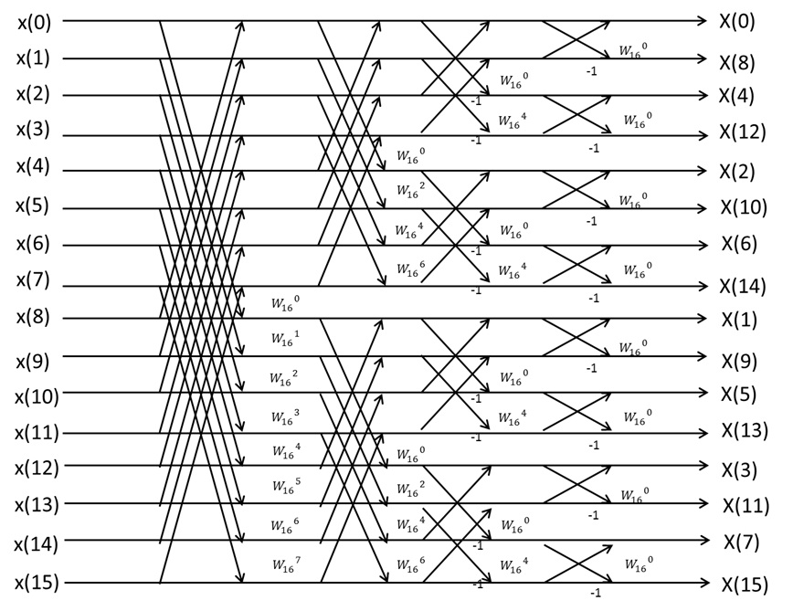 Figure 32: 16 points FFT architecture
A serial input signal is delayed and carried into Butterfly arithmetic circuit. Then, system separates output signals of Butterfly processing circuit into required signals for calculating FFT and no required signals by using Multiplexer.
After that, required signals are carried into next Butterfly arithmetic circuit. A circuit which we have made is shown by figure 34.
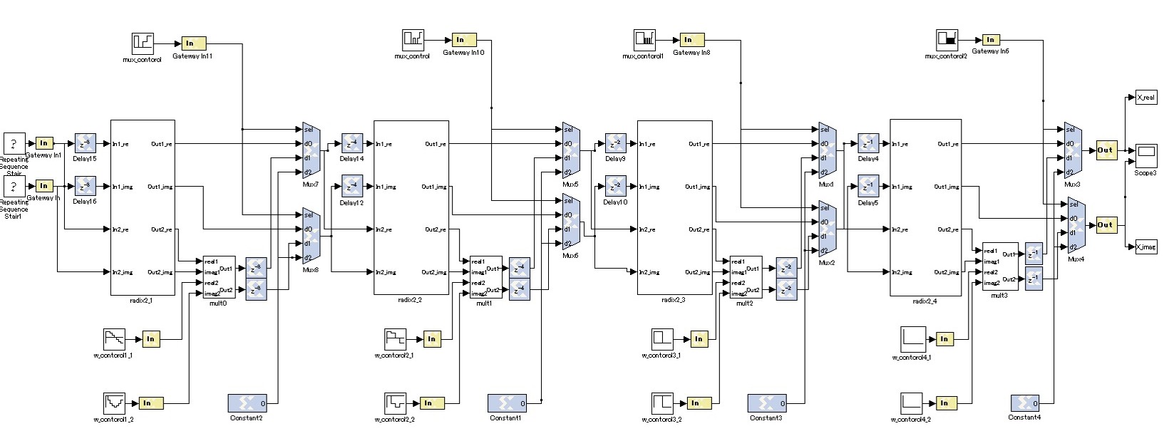 Figure 34: 16 points FFT circuit for serial input
1) MUX_control
MUX Control block controls input signal carried into selector of multiplexer. Output signal of Multiplexer is decided by this control.
The sequence parameter is shown by figure 35.
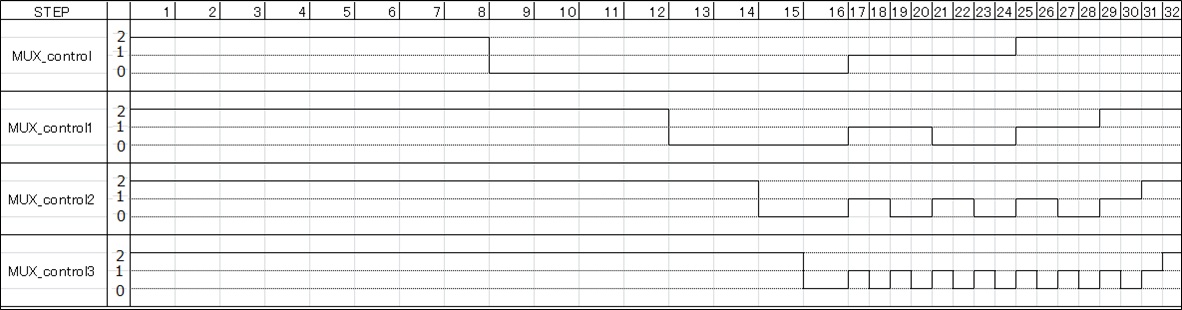 Figure 35: MUX_control sequence parameter
In figure 35, output signal from MUX_control varies on each step. The only signals required for FFT are sent to next Butterfly arithmetic circuit by the signal varying.
2) W_control
W_control is sequence representing twiddle factor W.
Butterfly arithmetic is done by varying W complex multiplied on each step.
Each W are…![]() ,
, ![]() ,
, ![]() ,
,![]() ,
, ![]() ,
, ![]() ,
, ![]() ,
,![]() Sequence parameters are shown by table 9.
Sequence parameters are shown by table 9.
Table 9: W_control sequence parameter

In Table 9, ![]() is expressed as 0.7071,
is expressed as 0.7071, ![]() is expressed as 0.9239 and
is expressed as 0.9239 and ![]() is expressed as 0.3827.
is expressed as 0.3827.
In Figure 30, as will be noted from the Table 9, first step on MULT0 is multiplying by ![]() and the next steps are multiplying by
and the next steps are multiplying by ![]() ,
, ![]() ,
, ![]() ,
, ![]() ,
, ![]() ,
, ![]() ,
, ![]() in order. First step on MULT1 is multiplying by
in order. First step on MULT1 is multiplying by ![]() and the next steps are multiplying by
and the next steps are multiplying by ![]()
![]()
![]() in order. First step on MULT2 is multiplying by
in order. First step on MULT2 is multiplying by ![]() and the next step are multiplying by
and the next step are multiplying by ![]() All steps on MULT3 is multiplying by
All steps on MULT3 is multiplying by ![]()
Timing diagram of 16-points FFT circuit for serial input is shown in Figure 36.
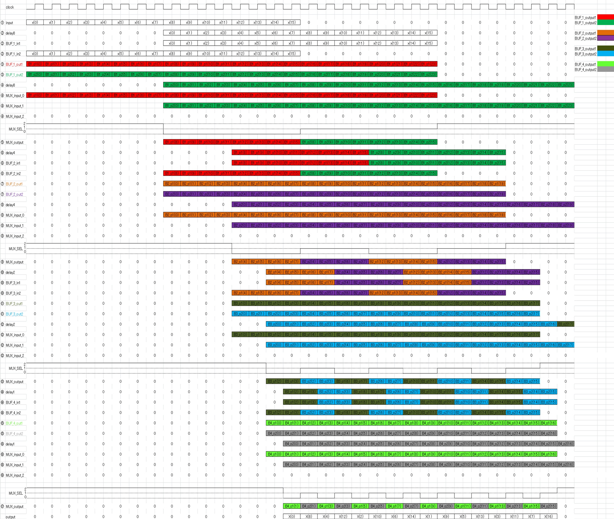 Figure 36: Timing diagram of 16-points FFT circuit for serial input
(2) Verification
A simulation result for input signals that x(0)=0+0j, x(1)=1+1j, x(2)=2+2j, x(3)=3+3j, x(4)=4+4j, x(5)=5+5j, x(6)=6+6j, x(7)=7+7j, x(8)=8+8j, x(9)=9+9j, x(10)=10+10j, x(11)=11+11j, x(12)=12+12j, x(13)=13+13j, x(14)=14+14j, x(15)=15+15j is shown in Figure 37.
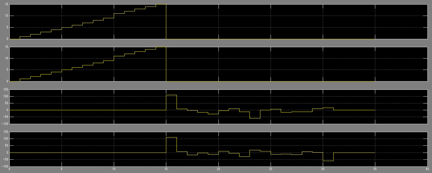 Figure 37:
Calculation results on MATLAB and the errors are shown in Table 10.
Figure 10: Output waveform of 16-points FFT circuit for serial input

By Figure 37, the Latency between an input and an output for this circuit is 15.
The verification of 16-points FFT circuit is making m-file for test, and calculation of mean square error (MSE) between result on MATLAB and result for circuit by random inputs a hundred times. The result is shown in Table 11.
Table 11: Calculation result of MSE

By the Verification, this 16-points FFT circuit perform that MSE of real part is  、 and image part is
 ![]()
5. Expansion method for 32-points or 64-points FFT
By the same expansion token, serial inputs are delayed and inputted into butterfly circuit, and only necessary outputs for FFT are inputted into next butterfly circuit. It is possible for the expansion by the control on Mux. In this way, Radix-2 ![]() -points FFT circuit can be designed. Furthermore, also Radix-4
-points FFT circuit can be designed. Furthermore, also Radix-4 ![]() -points FFT circuit can be designed.
-points FFT circuit can be designed.
6-1. Level1 :[128-point FFT]
In this level, designner must assume input signal coming in serially with HEAD signal as shown in figure 39. Design FFT circuit which generate FFT outputs and OUTHEAD signal with some latency. The latency is arbitrary.
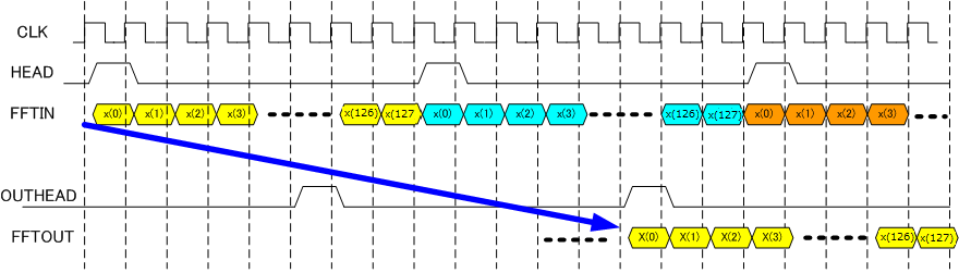 figure 39: Task waveforms
Table 5: Pin list
|
FFT |
|||
| Signal name | in or out | bit width | explanation |
| CLK | IN | 1 | Clock |
| HEAD | IN | 1 | ‘1’ means the beginning |
| FFTIN_I | IN | 8 | Input Real components (Unsinged Int,0-255) |
| FFTIN_Q | IN | 8 | Input Imaginary components (Unsinged Int,0-255) |
| OUTHEAD | OUT | 1 | ‘1’ means the beginning |
| FFTOUT_I | OUT | 14 | Output Real components, Keep 8-bit precision |
| FFTOUT_Q | OUT | 14 | Output Imaginary components, Keep 8-bit precision |
6-2. Level2: [16,64, 128-point FFT]
This should be implemented by only one circuit.
7. SPEED and AREA
Although it is getting very difficult to compare many designs, please use the following design parameter normalization.
The UNIT AREA is defined as 50 inputs EXOR circuit.
The UNIT SPEED is the latency of 50 inputs EXOR circuit.
Please show your design’s area and speed by this normalized UNITS.
50 inputs exor VHDL:parity.vhd
8bit Input (Unsigned Fixed point: Arbitary Decimal Point)
Source:
RSS Links

Blogs I Follow
Top Posts & Pages
Image

RSS

Embedded System
 Học Để Làm
 RoMeLa
 Học AVR
IC Design & Manufacturing
 siliconrun
Scholarship Infomation
Nano Technology
 Nano Hub Project
 Nano Hub University
Global University
.jpg) Open Uni
Open Uni Uni of Oxford
 FPGA
FPGA
- An error has occurred; the feed is probably down. Try again later.
